VLSI Design & Verification Internship - 3 Months
VLSI Design Internship in Patna Bihar - 3 Months ₹999. Learn Verilog, SystemVerilog, RTL design, and verification.
Program Description
Skills You'll Learn
Projects You'll Work On
VLSI Design Project
Design and verify a complete digital system using Verilog/SystemVerilog and implement on FPGA
Program Modules
W1: Digital Design Fundamentals
Combinational logic, sequential logic, FSM design
W2: Verilog HDL
Verilog syntax, modules, testbenches, simulation
W3: SystemVerilog & Verification
SystemVerilog, assertions, coverage, UVM basics
W4: RTL Design & Synthesis
RTL coding, synthesis, timing analysis, optimization
W5: FPGA Implementation
FPGA design flow, place and route, hardware testing
W6: Final VLSI Project
Design and verify a complete digital system on FPGA
Key Features
What You'll Learn
Examination Details
| Exam Name | Full Marks | Pass Marks |
|---|---|---|
| Project Evaluation | 100 | 40 |
Internship Details
Prerequisites
- Pursuing or completed Diploma/BTech Electronics/ECE
- Basic digital electronics knowledge
Who Can Enroll ?
- Electronics Engineering students
- ECE students
- VLSI aspirants
- Semiconductor professionals
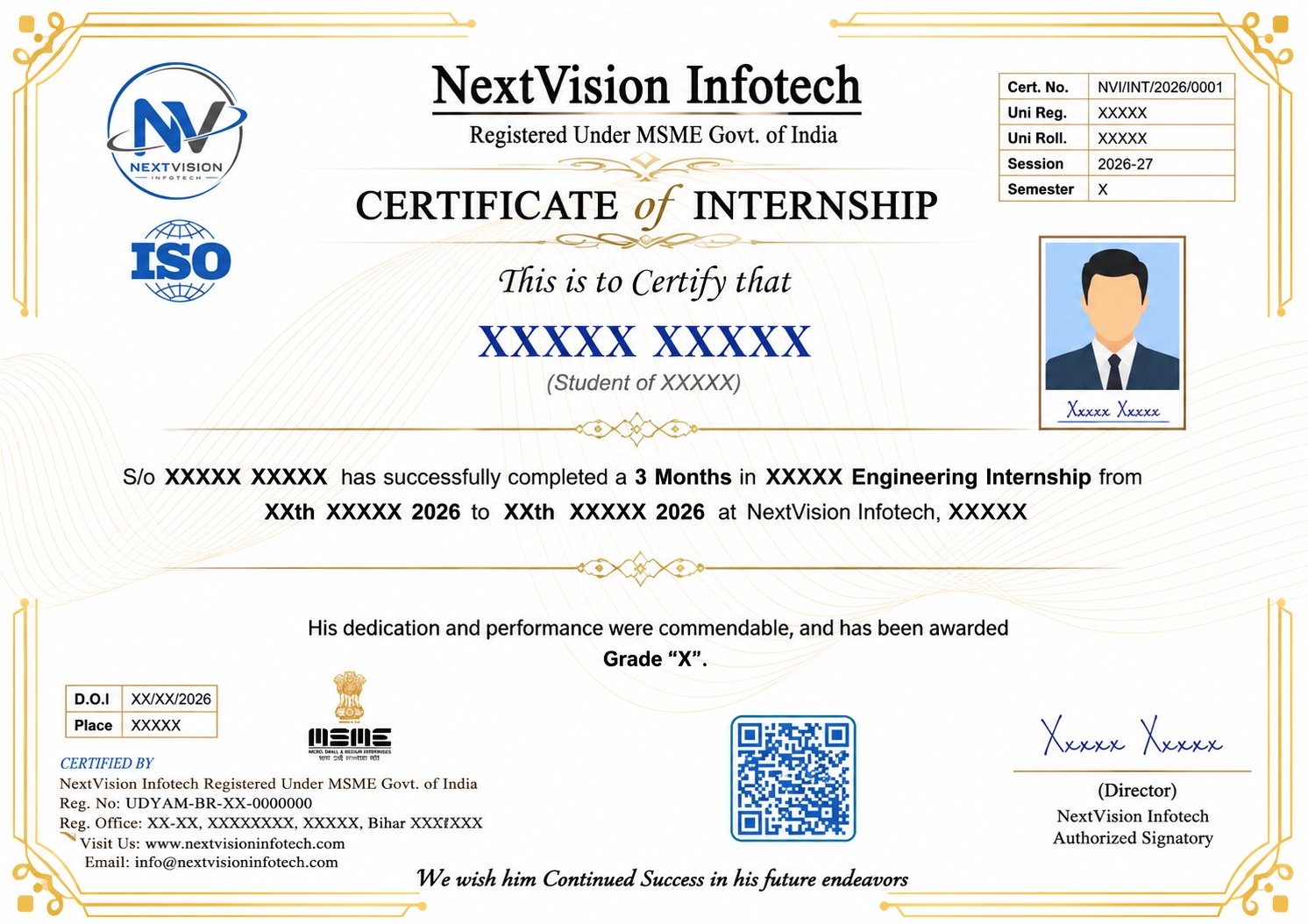
Certificate Preview
Related Internships
You might also be interested in these
Electronics Engineering Internship - 1 Month
Electronics Engineering Internship in Patna Bihar - 1 M...
Electronics Engineering Internship (Quick Industrial Training) - 15-Day with Certificate
Electronics Engineering 15-Day Internship in Patna Biha...
Electronics & Communication Engineering Internship - 3 Months | 5G, IoT, Embedded Systems
Electronics & Communication Internship in Patna Bihar -...
Our Students Did It!
CHANDAN KUMAR
Internship Program
"Best decision I ever made! The teaching quality and practical training helped me land my dream job. Highly recommended! 🌟"

Abhay Kumar
Internship Program
"Amazing experience! The mentors are super supportive and the course content is industry-ready. Got my certificate with confidence! 💯"

Prashant Kushwaha
Internship Program
"NVI Gaya changed my career path completely. Practical projects, real-world skills, and expert guidance — everything was perfect! 🚀"

Simran Shree
Internship Program
"Learned so much in such a short time. The internship gave me real experience and confidence to face interviews. Thank you NVI! 🙏"

Shubhangi pandey
Internship Program
"Best decision I ever made! The teaching quality and practical training helped me land my dream job. Highly recommended! 🌟"

Shubham Chaurasiya
Internship Program
"Amazing experience! The mentors are super supportive and the course content is industry-ready. Got my certificate with confidence! 💯"
Ashmit kishore
Internship Program
"NVI Gaya changed my career path completely. Practical projects, real-world skills, and expert guidance — everything was perfect! 🚀"

Payal Mourya
Internship Program
"Learned so much in such a short time. The internship gave me real experience and confidence to face interviews. Thank you NVI! 🙏"

Samim Ahmad
Internship Program
"Best decision I ever made! The teaching quality and practical training helped me land my dream job. Highly recommended! 🌟"

Amogh Raj Singh
Internship Program
"Amazing experience! The mentors are super supportive and the course content is industry-ready. Got my certificate with confidence! 💯"
Our Certificate Samples
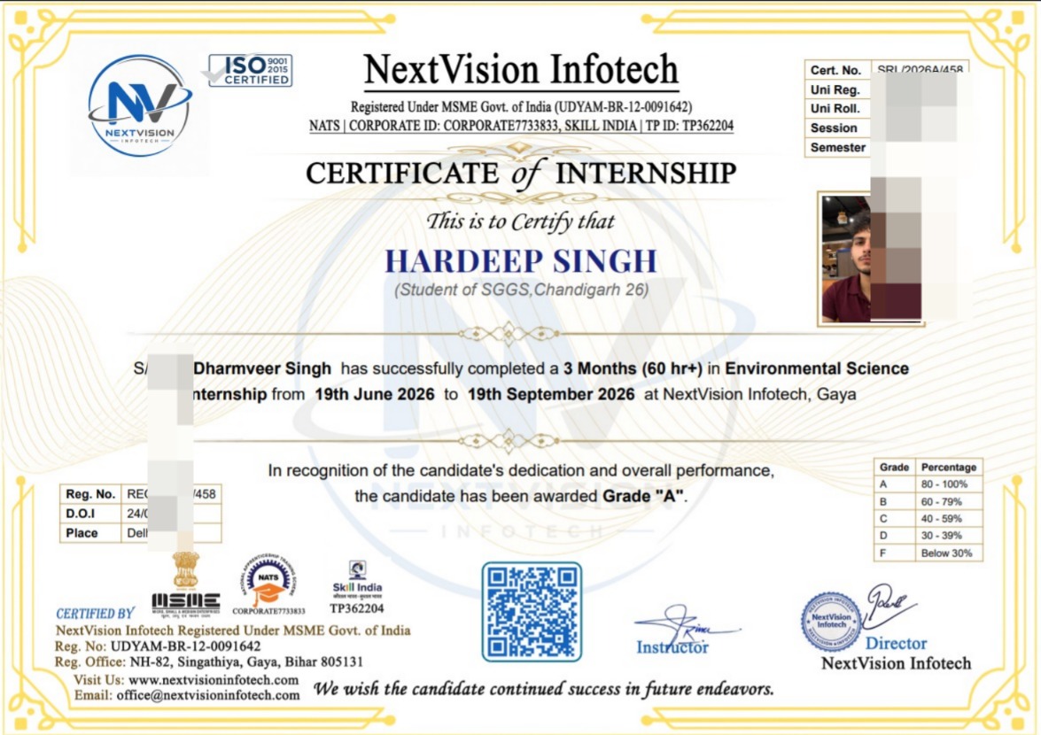
Internship Certificate
Tap to view
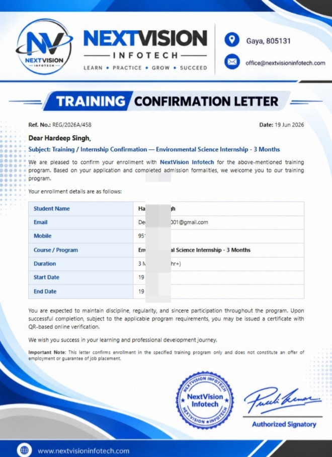
Joining Letter
Tap to view
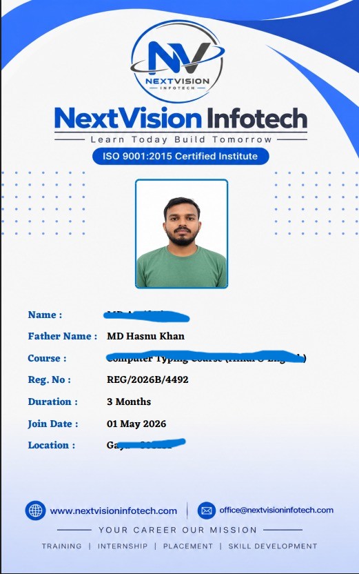
Student ID Card
Tap to view
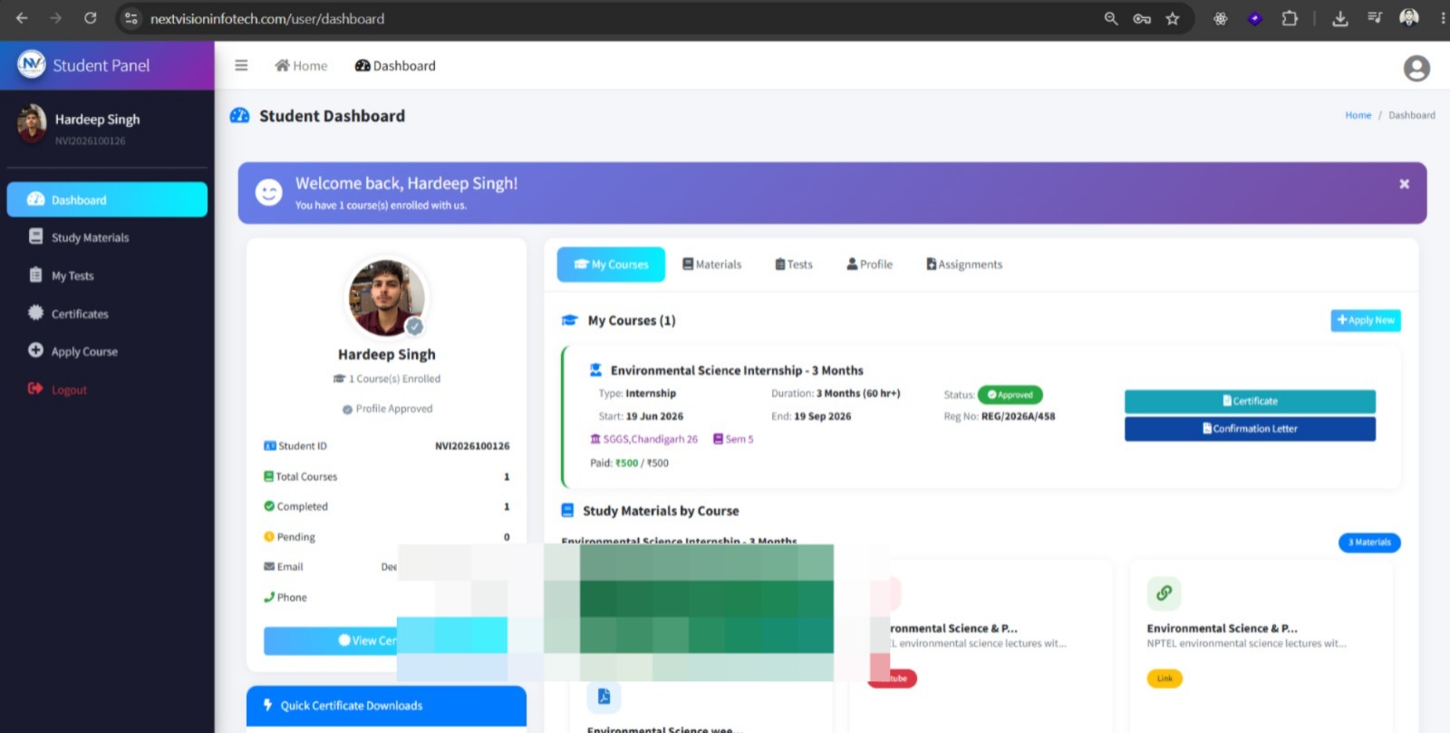
Student Panel
Tap to view
All certificates are issued by NextVision Infotech & are verifiable upon request.
Ready to Start Your Journey?
Take the first step towards your dream career with our internship programs